
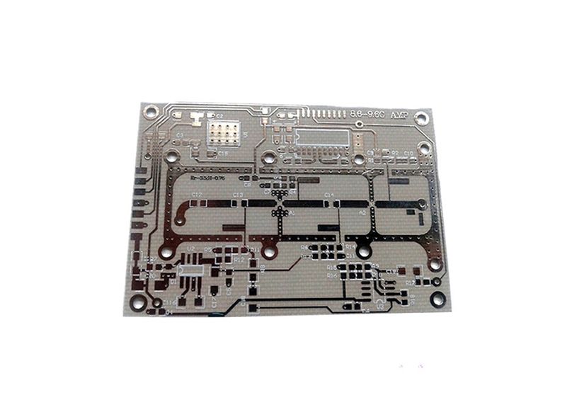
Finished copper on the traces is 18–25 µm. Heavy-copper areas change the etch and the imaging recipe, and they are worth flagging before the panel is booked rather than after the first lot.
18–25 µm plated copperWhat matters on an HDI board is not whether we have a certificate on the wall. It is which acceptance class your board is being built to, and how we prove it before it leaves the building.
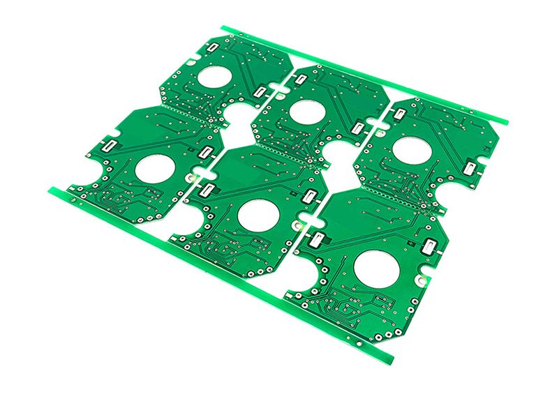
Class 3 is not a grade we assign ourselves. Your drawing specifies it, and the annular ring, plating thickness and inspection frequency all change with it — which changes the price.
Inspection on an HDI board has to happen during the buildup, not only at the end. A via that was filled badly is invisible once the next layer is laminated on top of it.
A microvia that fails does it after thermal cycling, not during electrical test. Copper fill quality and barrel integrity are what decide it, so those are the process controls we hold tightest, and IST thermal cycling is available as a qualification step.
Read this before you take the list above as a claim
This site is a design sample built on a placeholder brand. No certificate number is published here, and nothing on this page should be read as a claim that Nordvia Circuits holds any of these certifications. Certificate copies are provided with a real quotation.

Finished copper on the traces is 18–25 µm. Heavy-copper areas change the etch and the imaging recipe, and they are worth flagging before the panel is booked rather than after the first lot.
18–25 µm plated copper
Mask colour sets the contrast the inspection system works against. Green and red give the imaging the most headroom; black and matte finishes need a different recipe and are worth flagging up front.
Set the AOI recipe earlyEngineering reply within 12 hours