
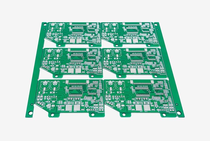
Panel array
Step-and-repeat panels with tooling strips both sides. Panel utilisation is where the HDI premium gets paid back.
Sequential lamination from 1+N+1 to 7+N+7. Drilling a small hole is not the hard part. Keeping a stacked via tower one solid copper column after thermal cycling is.
↓ Below is this board in section · six layers · 1.0 mm overall
These are the shapes that actually come through: panel arrays, long strips with edge connectors, castellations, metal-core modules, rigid-flex tails. If your board looks like one of these, the stackup conversation is short.
Step-and-repeat panels with tooling strips both sides. Panel utilisation is where the HDI premium gets paid back.
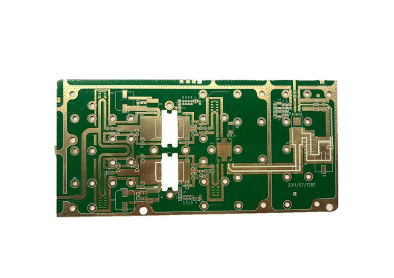
Long, narrow, gold-finger edge. Registration across that length is the thing that decides yield, not the layer count.
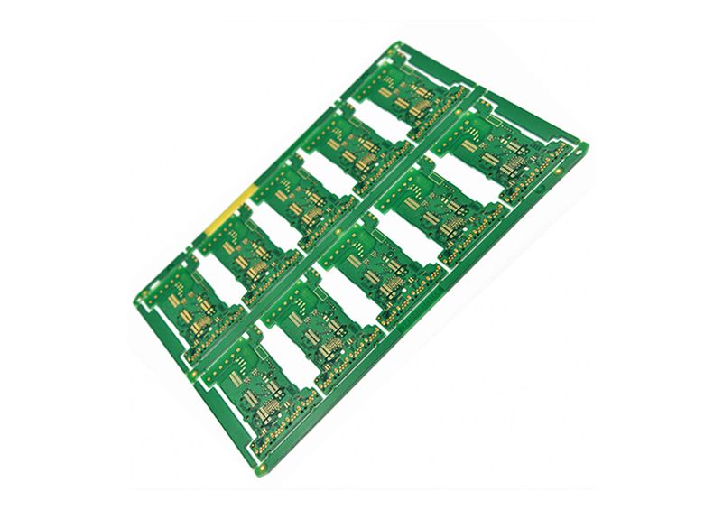
Six-up strips for pick-and-place. Small boards utilise a panel better, which is one of the few places HDI beats conventional on price.
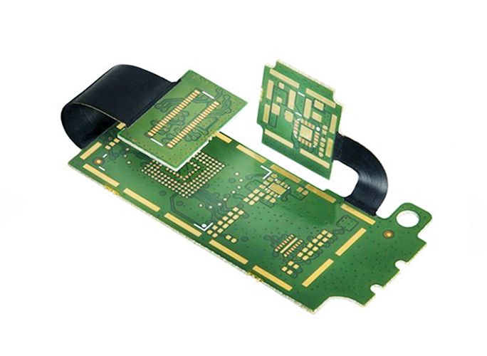
Routed outlines, castellations, cut-outs. Worth telling us early — odd-form changes the routing and the fixture, not the stackup.
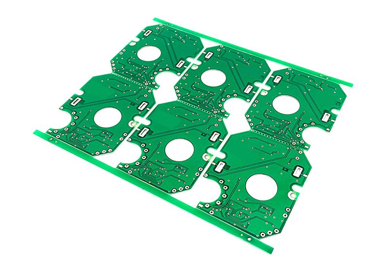
Several designs on one panel. When two boards share a stackup, quoting them together is usually cheaper than quoting them apart.
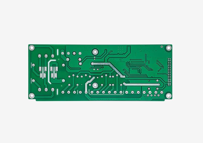
0.4–1.0 mm overall with 50–75 µm dielectric per layer. This is the shape most HDI projects actually arrive in.
Your BGA pitch decides it. At 0.8 mm and above, a conventional multilayer board is usually cheaper and faster. At 0.65 mm and below, microvias stop being an option and become the premise.
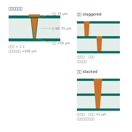
A CO2 laser cannot cut through copper, so the copper window has to be opened first. A UV laser at 355 nm cuts both copper and dielectric and is what we use below 100 µm. Three steps after that are not optional: desmear, electroless copper seed, pattern plating to fill.
Then it gets planarised. Coplanarity is held inside 3 µm. Skip that and the next prepreg presses down over the via bump and seals air above it — a void you will never see.
Finished via ≈100 µm dia · 60–75 µm deep · top 75 µm tapering to ≈50 µm · aspect ratio < 1:1
Stacked microvias
Consecutive microvias line up into a tower. Without bottom-up copper fill there is nothing for the next layer to land on, so fill and planarisation are part of the structure rather than a finish. Highest density, and the step that most often decides the price.
Staggered microvias
Each via offsets from the one below, so no copper fill is required. The cost is routing area, not reliability. On most boards this is what the stackup should use by default — reserve stacked vias for the areas where density genuinely binds.
Core fabrication, buildup and through-hole drilling do not share a registration budget. That is the whole reason a board goes to one line rather than another, and it is what the numbers below are really about.
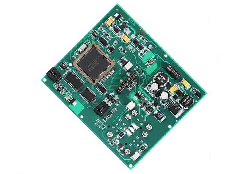
Holding ±25 µm across a buildup layer is a discipline held on every panel. The laser is the same on both lines; the inspection frequency is not.
±25 µm HDI budgetMicrovias in the buildup layers, mechanical through-holes for power and ground. Most HDI designs are hybrids, and that is the cost-effective way to build them.
Two via types, one board
Via structure feasibility, aspect ratios and capture pad sizes are checked against your design before production. DFM comments come back with the quote, not with the first panel.
Before the panel is bookedBuildup dielectric runs 50–75 µm against 100–200 µm on a conventional board. At the same target impedance that means narrower traces, so the stackup model belongs in the quote request, not in the follow-up.
Engineering reply within 12 hours