
Request a quote
Capabilities

Check your board against the list.

Everything on this page is a line you can hold us to. If your design sits inside these numbers, we can quote it. If it sits outside, say so early and we will tell you what changes.

7+N+7Max build-up
30Max layers
75 µmMin laser microvia
3 / 3 milMin trace / space
What those numbers look like

Capability lines are easy to read and hard to picture.

These are boards that sit inside the limits above — thin stacks, panel arrays, strips with edge connectors, castellations, metal-can modules. The point of showing them is that you can tell at a glance whether your own board belongs in the same family.

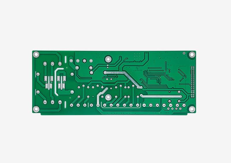
Thin green circuit board with fine trace routing, on a white background.
Thin stack

0.4–1.0 mm overall. Buildup dielectric 50–75 µm per layer.

4–8 layers typical
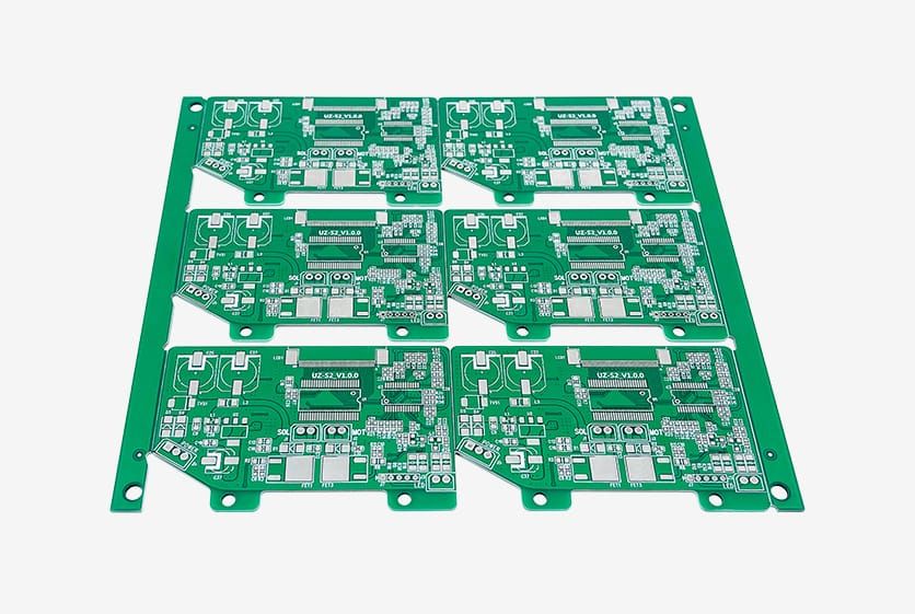
Panel of repeated identical circuit boards after routing.
Panel array

Step-and-repeat with tooling strips. Panel utilisation is a cost lever, not a detail.

Tooling both sides
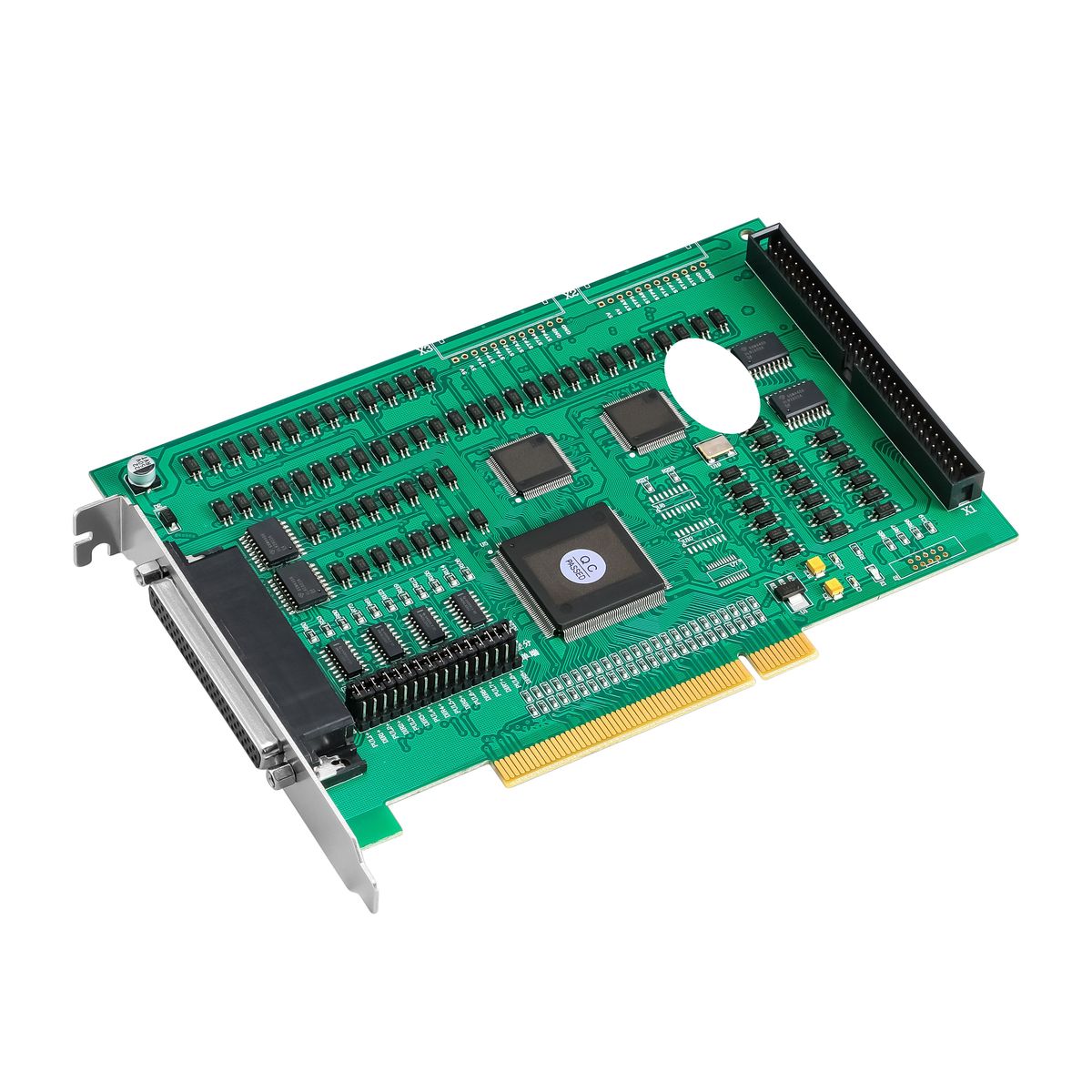
Circuit board with gold-plated edge contacts, viewed from above.
Edge connector

Gold fingers with a controlled bevel. Length is where the registration budget gets tested.

ENIG or hard gold
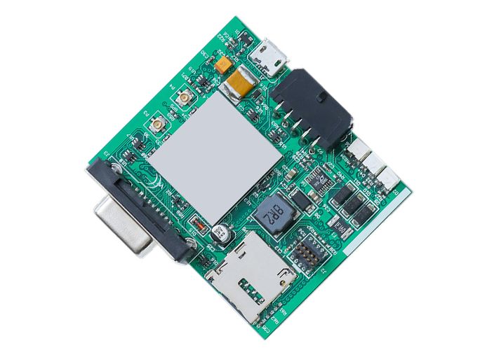
Module board with a metal shield can and dense routing underneath.
Shielded module

A metal can over a dense area means via-in-pad and a tighter escape pattern underneath it.

Via-in-pad required
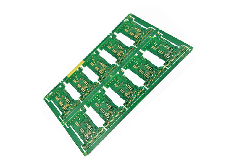
Six small identical circuit boards joined in a strip.
Small-board strip

Six-up for pick-and-place. Small boards utilise a panel better, which offsets some of the HDI premium.

Better utilisation
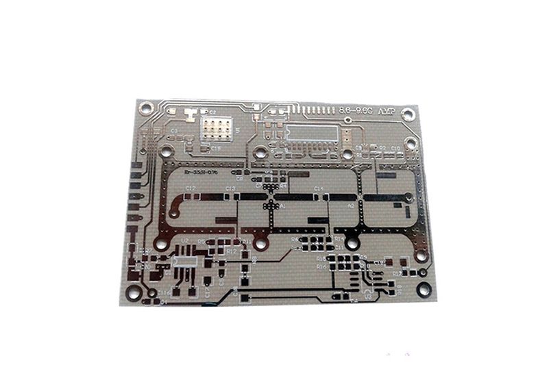
Two-layer FR-4 circuit board with wide traces, on a white background.
Conventional, for contrast

This is what 4/4 mil and a 200–300 µm mechanical via look like. If your board fits here, HDI is overkill and we will say so.

Not HDI
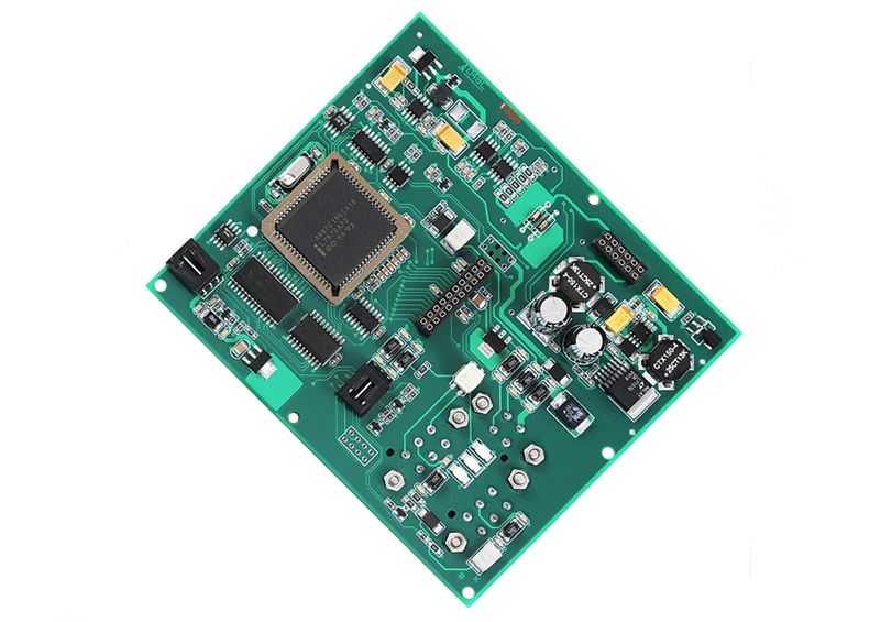
Square circuit board with a fine-pitch IC package in the centre.
Fine-pitch escape

Dense pad arrays under a single package are what force microvias in the first place.

0.4–0.65 mm pitch
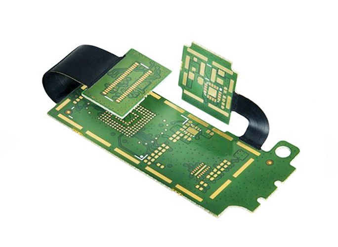
Octagonal circuit board with castellated edges and a central cut-out.
Odd-form and castellation

Routed outlines and castellated edges change the routing and the fixture, not the stackup.

Tell us early
Build-up and layer count

Build-up steps, and what each one buys you.

1 step · 1+N+10.65 mm BGA · 4–30 layers8 days prototype
2 steps · 2+N+20.5 mm BGA · 6–30 layers10–11 days
3 steps · 3+N+30.4 mm BGA · 8–30 layers13–14 days
4 steps · 4+N+4Any-layer interconnect · 10–30 layers16–17 days
5 steps · 5+N+5SiP / AI accelerator · 12–30 layers19–20 days
6 stepsHBM / AP substrate · 14–30 layers22–23 days
7 stepsHighest density offered · 14–30 layers25–26 days
Vias

What we can drill, fill, and hold flat.

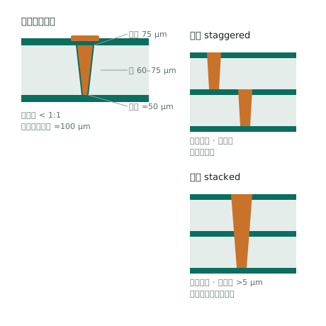
Microvia cross-section showing a 100 µm via tapering from 75 µm at the surface to about 50 µm at the capture pad, next to stacked and staggered via structures.
Aspect ratio is held below 1:1 in every buildup layer. Stacked vias are copper-filled and planarised; staggered vias are not filled.
Min laser microvia75 µmStandard production
Typical HDI microvia100 µmReliability margin prioritised
Advanced substrate level50 µmUV laser, DFM review required
Via depth, one dielectric60–75 µmAspect ratio below 1:1
Via-in-padCopper-filled, plated over, planarisedNo dimple above 5 µm
Blind and buried viasAvailable — blind outer to inner, buried inner onlyStandard
Resin-filled through-holesFlat, cappable surface for plating overStandard
Trace, copper, registration

How fine the routing can go, and how stable it stays.

Minimum trace / space3 / 3 mil (75 / 75 µm)Design rule
Minimum via pad250 µm (10 mil)Design rule
Plated trace copper18–25 µmPattern plating
Layer-to-layer registration±25 µm on HDI buildup · ±50 µm conventionalPer lamination cycle
Materials and thickness

Buildup dielectric, matched to your stackup model.

FR-4 prepreg 10802.8 mil curedStandard buildup
FR-4 prepreg 21164.6 mil curedStandard buildup
Panasonic Megtron 6R-5775 · Df 0.004 at 10 GHzLow-loss buildup
Isola 370HRTg 180 °CLead-free reliability

Conventional builds run 1.0–2.0 mm. HDI stacks with thin dielectrics go down to 0.4–1.0 mm, which is usually why HDI is chosen in the first place. Buildup dielectric runs 50–75 µm against 100–200 µm on a conventional board — at the same target impedance that means narrower traces, so bring the stackup model to the quote rather than after it.
Portrait photograph of circuit boards and electronics on a work surface.
Board thickness is a stackup decision, not a finishing option. Tell us the target early.

Outside any of these numbers? Send it anyway. A board that needs 50 µm microvias or 8 buildup steps is a DFM conversation, not a rejection.

Engineering reply within 12 hours