
What counts as HDI, in numbers.
A board is HDI when wiring density per unit area is higher than a conventional multilayer board can reach. In practice that means four things, and all four are measurable.
Microvia ≤ 150 µm
Trace / space ≤ 75 µm
Via pad down to 250 µm
Built by sequential lamination

Where the two constructions actually differ.
1+N+1 is the usual entry point, not the low end.
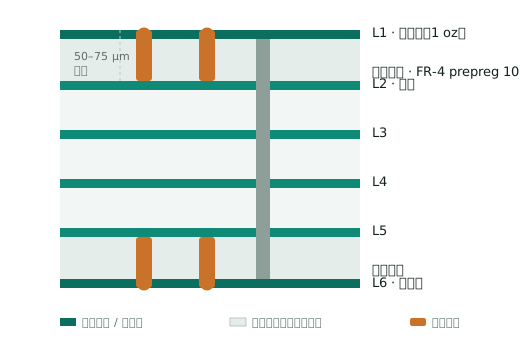
N is the core. Type I builds one microvia layer on each side of a 4-layer core and lands at 1+4+1 = 6 layers. Only the two buildup layers carry laser microvias; the core still uses mechanical through-holes. Two via types on one board is the norm, and the cheapest way to do it.
0.65 mm BGA
0.5 mm BGA
0.4 mm BGA
0.3 mm BGA
Stacked or staggered — this is where designs get expensive.
Stacked
Consecutive microvias line up. Copper fill is mandatory: without it the tower has nothing to stand on. Highest density, highest cost, and required for via-in-pad under fine-pitch BGA.
Staggered
Each via offsets from the one below. No copper fill needed. Cheaper, but it consumes routing area. For most boards this is the right default.
Put stacked vias only where density actually binds. Mixed via types on one board is normal, not a compromise.
Four things move the price. Board size is the last of them.
We do not publish unit prices. Fill the four rows in against your actual design and you will see where to stop — often it is cheaper to relax 3 mil back to 3.5 mil and buy another prototype round.
Not sure which type your board lands in? Send the Gerber and your BGA pitch. We will come back with the type, the step count, and the layers that will hurt.
Engineering reply within 12 hours